Wafering and Material Processing

We offer a finishing and manufacturing of brittle-hard materials for customers from various industries. The core areas of our R&D services are silicon crystal processing and the plasma treatment of wafers. In the field of silicon crystal processing, we offer all processing steps from mono or multicrystal to cleaned and inspected wafers. The manufacturing processes are not limited to silicon. Sawing of silicon carbide or sapphire is also possible.

Companies with a focus on wafer production or material processing are to be addressed by our range of services.


We offer:   

  • Processing of hard-brittle materials
  • Wafering (diamond wire and slurry process) of silicon, silicon carbide, silicon nitride and sapphire


Sensor-Supported Wafer Production

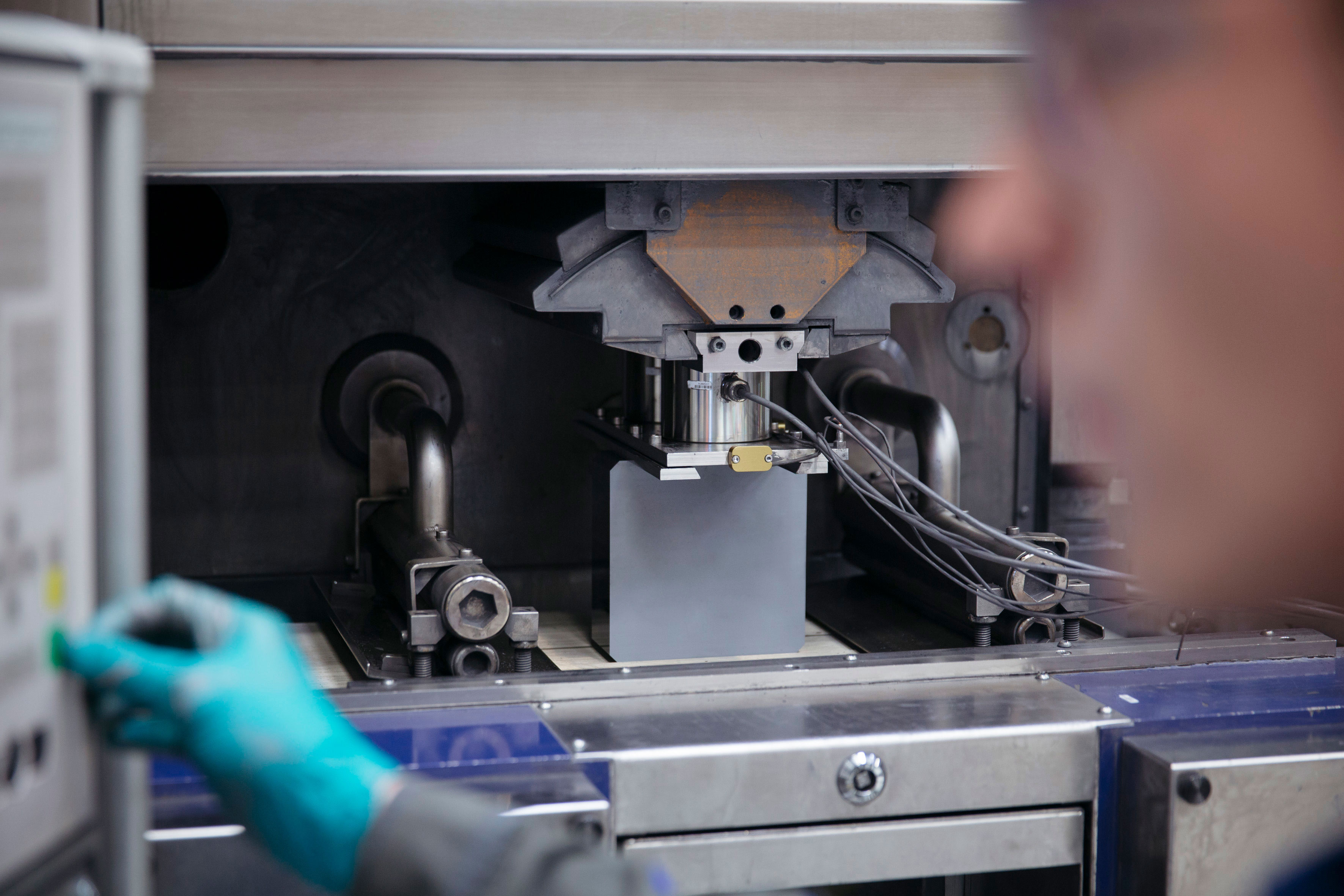
How do process parameters and consumption media influence wafer production? In order to determine the interaction between wire and workpiece, the multi-wire saws from Fraunhofer CSP (Meyer Burger DS264 & DS265) were equipped with force sensors.


Silicon Carbide Wafer Production

The multi-wire saw technology originating from the semiconductor industry has been successfully transferred to other branches of industry and materials.

Sawing process
© Fraunhofer CSP
Sawing process
  • Charge carrier service life and resistance measurement on blocks | SemiLab WT-2000P
  • IR radioscopic system for the identification of SiC/SiN inclusions in blocks | Intego FRA 1307
  • Surface and bevel grinding | Okamoto type SIG 154 H
  • Cutting and squaring of mono- and multicrystals | Meyer Burger BS805
  • Wafer production (industry standard) | Meyer Bruger DS264, Meyer Burger DS265 (sensor monitoring)
  • Batch wafer cleaning | UCM6 (ultrasound cleaning system)
  • Inline measuring system with sorting unit for wafer end control and classification | Hennecke Type He-WI-03
  • Media consumption measurement (power and cooling) | Johnson Controls and FRAKO